Quantcast
Channel: DuWayne's Place
Viewing all 112 articles
Browse latest View live

An AD8307 power meter

$
0
0
When I started on the SPECAN spectrum analyzer, I purchased several AD8307 log detectors.
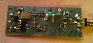
I found several slightly different designs for power meters, but most are basically the same with different output circuitry.  I decided to stay with the circuit used by Farhan in his Sweeperino and Specan.  Only change I made was to use 33uf molded RF chokes instead of resistors to feed the +5v and bring the  output from the detector to the outside of the shielded compartment.
After deciding on that I took a look at the Arduino software used to read the log detector and convert to dB.  There are several different methods used, some very simple and others that require rather complicated calibration schemes.  
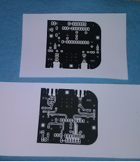
The best way  to test these would be to build a simple power meter.  I had the layout for the power meter part of the SPECAM and the Arduino and display that I had done for the Dummy Load Wattmeter.   Removing the dummy load portion of that board I was able to import the AD8307 power meter circuitry with only a little change  in the original layout.  For the Arduino Nano and Pro-Mini projects I use low profile IC sockets.  Since I want to move to more surface mount designs.  I changed the board layout to have solder pads for the Arduino and display sockets instead of using through hole. 
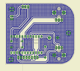
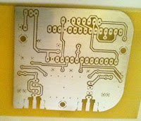
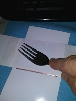
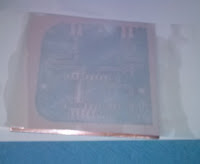
I etched up a double sided board, with the bottom being solid except for an isoleted block under the AD8307 circuitry.  I had a little problem and the board was over etched, with a lot of pin holes in the ground plane area on both sides.  I flowed a layer of solder over the board to cover some of them.  After populating the board, I cut a .25" wide strip of .020" circuit board material to use as a shield around the log detector circuitry.


I was able to use much of the software from the DL Wattmeter.
I tried several of the chunks of code for the AD8307 interface, and finally went back to Farhan's basic code.  It is one of the simplest and gives results that will be more than adequate for most amateur use.  It does not have a calibration routine, so a cal value has to  be put into the source code.  After only a couple tries comparing the readings with that of the wattmeter function in the Chinese SNA I found a cal value that gave readings within 1 dB of the SNA.
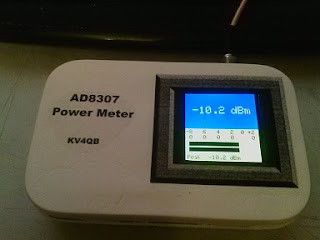
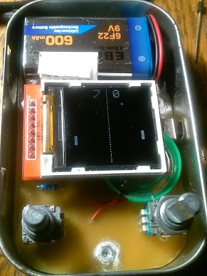
I wrote the software to include the numerical value from the log detector and also have a analog bar display.   I find that a bar display is often easier to use when aligning equipment.  I also added a little code to give another bar showing the peak value measured.  By implementing a counter in the main loop I was able to have the peak reset to the current level after 10 seconds from the last highest peak reading.      Next to put it in another Altoids tin. 

Looking around for a way to check the calibration, I found a simple RF power reference circuit on the web site of W1GHZ.  I had room on the same board as the power meter, so added that layout.  Will update after I finish building and test it. 


20 Mhz. power Reference & Calibrating the Ad8307 power meter

$
0
0
I had the AD8307 power meter working, and compared it against the Chinese SNA in watt meter mode.  The SNA has a built in step attenuator, using that I found the linearity to be very good.  Only thing I was not sure of was the accuracy of the calibration on the SNA.
Looking around the web I found several articles on using a CMOS crystal oscillator can and adjusting for a certain DC output level.  I really wanted something that I could just build and not have to worry about adjusting.  I  would also like to use one as an internal reference for the spectrum analyzer I am building.

 I found a circuit from W1GHZ that looked like it would do nicely. 

http://www.w1ghz.org/small_proj/small_proj.htm 

His circuit uses a crystal oscillator and then takes its output and feeds a pair of back to back diodes.  This should give a very accurate and stable output signal.  This is fed through a low pass filter to remove harmonics of the square wave to a attenuator to set the final output level at -10 dBm.


Looking around I found a 20 Mhz. oscillator that I had form another project.  I used ELSIE to design a 5 pole low pass filter using component values I had on hand.  A small circuit board was built using mostly surface mount components except for the two molded RF chokes in the low pass filter.  I made room on the board so I could parallel resistors and capacitors to make the values needed.  Checking the output level on my scope I fund the output to be around 208 mv. p-p  Close enough the the 200 mv. value for -10 dBm.

The method I used to compute dBm. from the ADC reading on the Arduino does not have a calibration routine.  The correct value has to be determined by trial and error, and entered into the sketch.

While I was trying to find the correct value I noticed something interesting.  When I had the AD8307 meter powered by a battery the reading was very constant. 


 But, when I powered it from the PC when I was uploading the sketch with a different cal value the reading jumped around quite a bit, and was much higher.  Indicating that a lot of noise was coupled from the PC to the power meter.  Having the battery connected at the same time greatly reduced the noise but did not eliminate it completely.  
This indicates that any test instrument powered from the PC might be the cause of noise found during testing.  Powering from battery if possible would probably be the better choice.

It only took me 3 tries at setting the calibration value to get the AD8307 meter to read within 0.1 dBm. of the -10 dBm reference signal.  Now I still need to cut up another Altoids tin to put the meter in.


Power meter and reference finished.

$
0
0
I finished up the AD8307 power meter and -10dBm reference. 

For the reference I soldered some .020 in double sided circuit board material around the outside edges to protect the components.  Since this will not be used very often I decided to not put in a switch, I just glued the assembly to a 9V battery holder.
I have a new circuit board layout with room for mounting holes that I will build for use as an internal reference in the Spectrum Analyzer I am working on.

After a little cutting and a lot of sanding and touch up work I painted and printed some decals for the Altoids tin I used to house the Power meter.

According to the readings on my oscilloscope the reference should be within 1 dBm of the desired -10 dBm.  After setting the calibration values in the Arduino sketch for the power meter, the readings are consistently within .5dBm.  Checking linearity with several in-line attenuators all readings were within 1dBm.

Without access to other calibrated standards, this is about as accurate as I can come up with, and should be accurate enough for checking most things an amateur would build. 
Now to get back to the spectrum analyzer build.


SPECAN 2nd IF filter UPDATED 11/4/15

$
0
0
Got back to work on the spectrum analyzer, with the 2nd IF filter board.     Revised 11/4/15

 This is two filters that are relay switched.  The narrow filter about 1Khz uses 9 crystals and has two in line amplifiers between each set of 3.  The wide filter should have about a 400Khz bandwidth and is comprised of 5 LC networks.


I did a board layout using mostly SMD components. During the layout of the narrow (1KHz.) filter, I found it would be easier to use leaded 2n3904s instead of the smd components.  Just too lazy to redo everything I had already finished to use the smd part.


I had ordered a batch of 30 12MHz. crystals, and using my SNA  to match them, I got 9 that were within about 100 Hz. of each other. 
After building this half of the board I decided to test and see what kind of a frequency response I had.


 Using the SNA jr. to check the bandwidth,I found the signal at just a few KHz. below 12MHz.  Narrowing the sweep range I found a nice peak and a bandwidth  of about the 1KHz. required.  From everything I have read, for a Spectrum Analyzer filter you want more of a peaked response than that for a SSB filter.  So this response looks like it will work.  After I finish the board I will check the responses with the Chinese SNA  that has  options for measuring bandwidth.  But, the SNA jr. is so easy to use on the bench it is what I usually go to when building.


Next to do the wide bandwidth filter.  I have not decided If I want to wind some toroids, or use some molded RF chokes.  If I use the chokes I had had added places for paralleling a couple of smd capacitors to tune to the correct frequency.  With the toroids I can try  to adjust spacing of the turns to help tune the filter elements.


I wound some toroids and tried to tune the segments by adjusting the coil spacing on the toroids.  This turned out to be a large pain, and I could not get them adjusted to the bandpass I wanted.
I had some 1.8uH molded RF chokes and some small 60pF trimmer capacitors that would fit on the board.  I  had placed pads for additional capacitors if needed, but found that I could tune the segments without adding any additional capacitors.

After finishing this filter I added the relay switching circuitry.  The relays I had were through hole, but I bent the leads and trimmed the length so I could solder directly to the elongated pads I had on the circuit board.

After completing I checked the bandpass filters.  The narrow crystal filter was about 1.1 kHz at 6dB. and the wide band filter was 456 kHz. at 6dB.

Just need to solder some .020" circuit board material as a shield around the assembly and on to the mixer stage.


S9 signal generator Updated 12/1/15

$
0
0
While waiting for some parts for the Spectrum Analyzer, I was looking around for a quick project.

There was a post on the QRP-tech yahoo group about the NorCal S9 Signal generator
http://norcalqrp.org/files/NorCal_S9_Assy_V1.pdf


This is very close to the circuit for the Elecraft  XG2 Receiver Test Oscillator

http://www.elecraft.com/manual/E740084%20XG2%20Manual%20Rev%20F.pdf


This looked like something that might be useful for testing the Spectrum Analyzer after I get it finished.  I decided to build a similar unit, using parts from both design.  Looking at the NorCal circuit, I saw that they used  20 and 14 db pads instead of the single 34 db pad used in the Elecraft model.  I went with the NorCal circuit and added switching around both pads to have options of 50, 10, 5, and 1 uv. outputs. 


I want to put the signal generator in an Altoids tin, so I used the same template as my AD8307 power meter as the basis for the board layout.  I have found that I get more consistent etching of the ground pour if I do it as a hatch instead of solid.  I plan on using  2 row .1" header strips with jumpers instead of switches, so I placed extended solder pads on the board.  This way I can just bend the bottom part of the header pins out to the side and solder directly to the top of the board.

Now to etch the board after I get back from a hamfest tomorrow.

 11/8/15


Well it was a little damp and chilly at the Hamfest, so I didn't stick around as long as I usually would.  This gave me plenty of time to etch the circuit board.  For SMD boards I have been using the blue press-n-peel transfer paper to eliminate etch through, and I get a cleaner pad for the SMD components.  I also let the boards sit in some "Liquid Tin" solution for about a minute to give a nice tin coating to the traces.  This seems to solder a little better than the bare copper.


I built the oscillator portion of the board to test how much output I was getting.  From the Elecraft document it looks like the oscillator should put out about -50 dBm before the attenuators.  Hooked mine to my home-brew AD8307 power meter and got a reading of -48dBm.  Checked the voltage to the oscillator and had about 1.6 volts, I might try adding another diode in series to drop the voltage  and see what that does to the output. 
Now on to the attenuators,  I am missing a one of the values for the 20 db pad but will try with the  closest value I have for now.  Will replace with correct value when the assortment of low value SMD resistors I have comes in. 

Since it is raining out I decided to finish the board and add the attenuator  components.  With the attenuator pads out I measured -68.2 dBm on my power meter.  I added another diode in series with the existing diode, this dropped the voltage to the oscillator to 1.07 volts.  Measuring the output with the additional diode I measured a value of -72.8 dBm.  This is more than close enough to the desired -73dBm output level of the Norcal S9 generator.


Only have two crystals in the circuit for now (3.561 and 7.030) will add others as needed.  Listening to the output on a receiver. The 50uv gives about a S7 reading, readings for other levels are below S1 but I can hear definite changes in the signal as I change attenuator settings.
Unfortunately I do not have any calibrated test equipment to verify the values I found.  But I believe the accuracy should be enough for testing the home-brew equipment I am working on. 


Link to dropbox for Eagle files and toner transfer image.

https://www.dropbox.com/sh/p6jdf2z4cg31ut1
/AAD0zL4tcr9kYS_v0HMFjzCza?dl=0 


I finished drilling some holes in an Altoids tin and and mounted the circuit board.  I also printed a simple instruction card showing the jumper settings for the different signal frequencies and attenuator settings.  I sized this to fit inside the top cover of the Altoids tin.


A PONG Game for Christmas

$
0
0
It is getting close to Christmas, and I need to come up with another present for my son.  He always says that when he was a little kid he had wanted a game system, instead he got a real computer.  He had been a programmer for a while so I guess it wasn't a complete waste.  I think it is time to finally get him a computer game.  Looking around I found a couple versions of the original computer 'PONG"  game for the Arduino. 
I chose  the project from http://michaelteeuw.nl/ 
that looked like it would be easy to port over to the hardware I have on hand.  And of course it would fit in an Altoids tin.
I had an OLED  like the display in my "Canned Frog", but it was two color instead of monochrome.  I had a small TFT display left over from the DL Watt meter project, so decided to use that.

Looking a the schematic, it was very easy to take the board layout from that project and modify it for use for the PONG project.  I was able to remove the Dummy Load and detector components from the board, and move the Arduino Pro Mini and display up towards one end of the board to give room for the two pots I needed for the game controls.  Only other thing was to bring out a pin to connect a small speaker.

After etching the board and installing the components, I started on porting the software to work with the TFT display.  The main advantage of the software I chose, was that it had used the Adafruit graphics library.  I had a compatible library for the TFT display I was using, so it was only took an hour or so to make the necessary changes to use this display.

Main changes was in the resolution of the display, and handling the different colors available to this display.  The OLED display has a clear() function that was used during the draw routine that was not available in the TFT library.  I tried to  replace this with a fillScreen(color) function. Unfortunately this was much too slow and there was a lot of jiter.  Instead of filling the whole screen, I used the fillRectangle(color) function to only clear areas that needed to be redrawn.  This was much faster, and greatly reduced the amount of jitter.  Just a couple of other changes of game play and the porting was finished.
The part of the project that took the longest was cutting and aligning the holes in the Altoids tin.

The N6QW Simple-Ceiver

$
0
0
I spent most of the holidays visiting relatives. and had quite a bit of time to work on something I had been thinking about doing for a while.  I have been following the development of the Simple-Ceiver that Pete N6QW has been posting on his blog.   N6QW.blogspot.com .  
Pete spends a lot of time going through the design of a DC receiver that is later converted to a single conversion heterodyne  receiver for 40 meters. He goes through the design using LTSpice to simulate each stage before he builds them.  This powerful tool allowed him to optimize the circuit design before melting any solder.
I have a bunch of 12 mHz. crystals left over from the IF amplifier for the Specan, so I could use the same frequency scheme that Pete used.  I plan on using a  version of the SI5351 VFO  I had  built for the "Canned Frog" transceiver.  Different from Pete's circuit I will use another clock output from the SI5351 for the BFO.

 Link to schematic at  https://www.dropbox.com/s/dersy23jgj6h37c/Simple-ceiver-schematic.pdf?dl=0


After drawing the schematic and getting it checked by Pete,  I did a single sided board layout using mostly surface mount components.  I did not have surface mount versions of the ICs for the AF amplifier so I did the layout with extended solder pads for the leaded components. Although I plan on using the SI5351 for the BFO, I decided to add the BFO oscillator to the board.   
Etched the board now to start building and testing the receiver, first the audio amplifier stages.


Cold Toner Transfer Circuit Baords

$
0
0
For years I have been using the toner transfer method for making circuit boards.  I have an old Brother printer and a Scotch TL902 laminator that have worked well for this.  One of the problems I have found with this method is that the type of toner you use is very important.  If I use real Brother toner, I get very good results for most of my boards. I have tried using generic toner cartridges that are about 1/3 the price, but have not been able to get very good results.  Another problem is with large ground plane areas, I have  had problems with etch through, and pin-holes showing up in these areas.

I recently saw a post on Instructables about using a chemical method instead of heat to transfer the toner to the circuit board material.
http://www.instructables.com/id/Heatless-cold-Toner-Transfer-for-PCB-Making/?ALLSTEPS


Since my Brother toner cartridge was just about out and I would have to order a new one fairly soon, I decided to give it a try.
Looking around all my painting supplies, for solvents I found a can of denatured alcohol. The original article used Acetone , which I did not have, but I had  some Xylene I had used for thinning and cleaning up some enamel I had painted.  

I printed up several copies of a board I need to etch using the generic toner cartridge.  Playing around with different mixtures of denatured alcohol and Xylene.  I found that a 4 to one 1 mix of alcohol to Xylene would soften the toner without causing it to smear instantly.  I tried the method as shown in the video with fairly good success, and then tried to modify the method a little.  Here is what I came up with.

With an eye-dropper I put enough of the mixture on a cleaned board to evenly cover the board.  Then place the printed paper on the board and moved it around to position it properly on the board. 
After it was positioned on the board, I used the eye-dropper to saturate the paper with more of the mixture.  You could see the paper becoming more transparent and clearly see the toner pattern.
I let this set for about 30 seconds, and then covered with a folded over paper towel.  I then placed another piece of circuit board material on top of the paper towel and applied pressure for about 2 minutes.  After that time I removed the top board, and used the rounded back of a fork to burnish, through the paper towel.  After  It looked like much of the mixtue had direied, I removed the paper towel and burnished the laser paper directly.  You could clearly see the toner pattern through the paper.  After a couple of minutes of that, I left everything set for a couple of minutes for the last of the mixture to dry.
After it was dry, I soaked the board in water for a couple of minutes, and removed the paper by lightly rubbing with my fingers.
The toner on the board looked nice and crisp, good adhesion all over, and no sign of smearing.  After etching the board, I found very nice traces, no problems where traces went between IC pins.
Also found nice smooth ground plane areas, with no etch through, or pin-holes.
Looks like I will be able to save a lot of money on toner, and finally retire the laminator.  Probably only used about a half a teaspoon of the mixture, so the remainder of the quart  cans of alcohol and Xylene I had around should last a very long time.

 
Just a couple of pictures of the boards done with this method.
 
The completed board, and a close up showing the sharpness of the etching , and nice solid ground plane area without pin-holes.


Now to get to doing something with these boards.


N6QW Simple-Ceiver Audio Amplifier testing

$
0
0
I finished building the audio amplifier stages of the Simple-Ceiver and with a speaker hooked up I got a response when I touched the amplifier input.  That is always a good sign, but I wanted to check to see how quiet the amplifier is and the frequency response of the amplifier.
For checking audio stages my favorite program is Visual Analyzer available at  http://www.sillanumsoft.org/

New-Mini-USB-2-0-3D-Virtual-12Mbps-External-7-1-Channel-Audio-Sound-Card-AdapterThis is a PC based software that uses a sound card as the instrument. Not wanting to blow up the sound card in my PC if I do something stupid I use a really cheap USB sound card I got on eBay. This also has the advantage that I can connect it to the computer near my work bench with a USB extender cable, and only have the small unit on the work bench.  I have also used the same card to build a digital mode interface.  The one I usually use is this model and is available for less than $2.00 with shipping.

http://www.ebay.com/itm/New-Mini-USB-2-0-3D-Virtual-12Mbps-External-7-1-Channel-Audio-Sound-Card-Adapter-/161161417325?hash=item2585f8126d:g:2LMAAOSwl8NVVVbp

Visual Analyzer software is a utility package of audio related functions.  It has an oscilloscope, AF Spectrum Analyzer, Signal Generator, Voltmeter, and several other functions I have not used.
With a little additional circuitry it can also be used as a ZRLC meter.


I connected the output of the sound card through a 2.2uF capacitor to the top of the 10 K volume control and the input across a load resistor instead of a speaker.
Setting the sound card to output a 1 kHz sine wave, I adjusted the  output level and gain pot to the point just below where I saw any clipping on the signal.  Then I changed the signal to Pink noise and set the spectrum analyzer to average 100 traces.  This makes a nice clean display of the frequency response of the amplifier.  As shown in the response curve, it is fairly linear to about 12kHz. and then falls off sharply to its low level at around 14.5kHz.
Still waiting for a couple of parts to arrive.  One of them is the 100mH inductor in the output filter of the product detector.  After these arrive I will do a plot of the complete Audio section.


Double sided cold toner transfer experiment

$
0
0
I was very happy with the boards I made using the cold toner transfer method, and wanted to see how it would work for dong two sided boards. 

 
 I had a small board I waned to make that has a full ground plane on one side.  I printed the toner patterns directly in Eagle, making sure to mirror the top side.  The best paper I have found for this is Color Laser Gloss from Hammermill.  It is much thinner than photo paper but has the same glossy surface, and is only about $15.00 for 300 sheets.  


I cut the patterns in  long strips, and trimmed the top pattern so it had about a 1" overhang from the  each side of the toner pattern.  Then using a strong back-light I aligned the two patterns and taped the top pattern to the bottom.  I then stuck a piece of paper in between the two patterns to
protect the bottom pattern while I worked on the top.

Using an eye-dropper I placed a small amount of the solvent on one side of the prepared board blank., and slid it between the patterns. After positioning the blank I applied a few more drops of the solvent on top of the paper and spread it around until I could clearly see the toner pattern through the paper.


When It was positioned where I wanted it I placed a piece of printer paper on top and covered with a piece of blank circuit board.  I applied pressure for about a minute to set the toner in position.  I then removed the blank board and first with the paper still in place I used the back of a fork to burnish the toner pattern.  After a little while the paper began to become more opaque.  Then I removed the piece of printer paper and continued the burnishing with medium pressure.  


 When it looked like all the solvent had evaporated from the paper, I turned it over , removed the piece of paper that had been there to protect the bottom toner pattern.  Carefully lifting the pattern slightly I put a few drops of solvent on the board blank and spread it around until even.  I added a little more solvent to the top of the paper until I could clearly see the pattern.  I processed this side the same way as I had the other.

 I checked the board and everything looked fine.  I found one or two small pinholes in the toner on the large ground plane area that I touched up with a marker.  After etching I drilled a couple of holes in the board to check registration.  The photo shows the same hole as seen from both sides of the board.  The registration was much better than I had ever been able to get using the hot method with a laminator.


Cold toner transfer and chemical dangers

$
0
0
After linking my two posts on the Cold Toner Transfer method to 
https://groups.yahoo.com/neo/groups/Homebrew_PCBs
there has been much discussion about the danger of the chemicals involved.
Some of these mentioned the effects of day to day heavy exposure found in some industries.  The amount of chemicals used in this method is minute in comparison.  I still have about a third of the 4oz. bottle of mixture I made up after doing 3 single sided and and 3 double sided boards. 


But .it is always advisable to take precautions when working with any chemical.  Even the most common such as dihydrogen monoxide can be dangerous under the right condition.
Years ago I made a simple air filter that I use when etching boards and soldering. It is very small and can be easily setup next to where-ever I am working.

  I had a broken 12 v brushless fan from an old computer.  I cut out the bottom of a disposable food storage container and glued the fan to the bottom, making sure the fan would draw air in through the container.  I then glued a 9 v battery holder to the side of the fan and wired up a switch.
To the back of the fan I attached two of layers of zeolite air filter material, with a single ply of a two ply paper towel between them.  The filter is just held on by twisted wires through the normal mounting holes in the fan.


Very simple and very low cost.  Only thing I had to buy was the air filter material  about $2.00 ( replacement air filter from a kitty litter box).
I can move it around between the soldering station, etching tank and board prep.


QRP SWR Meter UPDATED 3/14

$
0
0
The North Georgia QRP Club has been selling several small kits for the last few years.
One of them is a simple QRP SWR meter, but the small meters that were originally used are becoming hard to get and much more expensive then when the kit was first offered.
Several members of the group spoke to me about coming up with an updated replacement.


I had the Arduino and display circuit along with software I had used in the DL Power meter and the AD8307 power meter.  Using the board layout from these projects, I added a simple directional coupler and detectors built with a binocular core transformer.  With a slight change in parts placement it is possible to build in an Altoids tin.  Or with the display mounted vertically, it can be built in an aluminum project box.


I split the display area with a digital display of the VSWR value in the top half, and bar graphs with digital display of Forward and Reverse values in the bottom. I later added a warning message that would pop up if the VSWR is greater than 3 to 1.   This picture shows the layout I decided to go with. For initial testing I used a couple of variable resistors to input DC values into the Arduino , so values shown are percent of full scale.


After building the directional coupler and detector circuit I did some playing with the software to get a close approximation of the actual power readings.  Everything seems to be working well down to around 2.5 watts.  Below that SWR value starts to loose accuracy.  I am waiting on some different diodes to see if I can get everything working below that level.  If that does not work, I am thinking of changing the detector  to add a little DC bias to the detector diodes.

Here is a quick video of the meter as my auto tuner matches to my multi band antenna.
Will update when I get the new diodes, or have to change the detector circuit.


I gave the first prototype to a club member that has better test equipment than I for test.
After a few minor changes to the software most of everything looks good, except for power values below about 2 watts.  It looks like this is because of the non linearity of the diodes. used.  Tried different types of diodes, but non linearity remains.
I decided that I would add a diode compensated amplifier to rectify this. I was able to find enough room on the board for the op-amp and associated components.  Initial testing looks like the power readings remain accurate down to about 100mW.  Some more testing is requited, but looks like the design is finalized, now to write documentation and see about getting everything ready to do a sample run of the kit.


Sweeperino Jr. Part 1

$
0
0


Now that I have the SWR meter nearly finished, I want to get back to working on the spectrum analyzer.  I will need to build and align several filters that are higher in frequency than either the SNAJr. or the Chinese SNA cover.  Lookng at some posts by Asher Farhan on his blog, he has a simple SNA that he called the  Sweeperino.


 http://hfsignals.blogspot.in/p/sweeperino.html  


This uses the same AD8307 power meter I had used before and a SI570 for the signal generator.  His version has a 2 line LCD display for frequency and measured power level , and uses a pot for tuning. There is a PC program for doing a display of the sweep, same program is also used for the SPECAN display.


Since I was only interested in displaying the sweep while aligning filters, I did not need the display or tuning pot.  I wanted to save the last si570 I have on hand for the spectrum analyzer, so I used a Adafruit si5351 breakout board I had left from another project.

  The power requirements for the si5351 board and ad8307 are very low, and could be powered directly from the 5 volt output on the Nano.  I used some 100uH. molded RF chokes with additional filter capacitors to feed power to the 5351 and 8307 .  I had used this before in the stand alone power meter, and with shielding was able to get a -74 dBm noise floor.
When I built the power meter I found it was fairly difficult to solder the SMD parts without a solder mask, very easy to have shorted traces.  After I finished etching a double sided board, I decided to try adding a solder mask. 
I found two methods of doing solder mask at home, the simplest appears to be using UV curable paint.   I watched a You-Tube video that makes it look like it should be fairly easy.

https://www.youtube.com/watch?v=Vj_cdBZO1Tk

Other than the paint, the only other thing needed was a UV light source, although you could probably just take it out into the sun to cure.  Looking around for UV light sources, I found a small unit that is designed for use with UV curable finger nail polish.  This was under $10.00 and can be powered from a USB port or USB power cell.  This unit has a push button that turns the light on for 30 seconds at a time, this will make timing the exposure very easy.


I printed up a stencil of where I wanted the mask to leave bare copper on a plastic overhead projector sheet.  Then got everything all ready to give it a try. I did a couple of quick tests on some scrap board to get the exposure time down. About 2.5 minutes seems to give good results.


Using a small plastic card as a squeegee and a piece of plastic cut from a zip lock bag, I spread a thin layer of the UV paint on the board and aligned the stencil with the etched pads.  I exposed the board to UV light for 2.5 minutes, and then removed the stencil and the piece of plastic.  Using a paper towel with some rubbing alcohol, I cleaned off the un-hardened paint.  After checking the mask, I exposed the completed board for another couple of minutes to make sure everything was hardened.


The board looked pretty good, with only a small area where the mask came off the ground plane area.  Not as pretty as a commercial board, but looks like it will do what I want it to do.  Looking at the area where the SMD components for the power meter circuitry will go, everything looked very nice.  I think this will make it much easier to solder in the SMD parts using my hot air gun.  I used the same process and masked the bottom layer of the board.

Next to build up the board, and get the Arduino software working with this configuration.

SWR Power meter update

$
0
0
Because of a family emergency I had to make a two week trip to the winter wonderland I escaped from about 30 years ago.  I was not able to do much on the SWR Power meter I am working on that the local QRP would like to kit.  I was able to get back in time to get a board stuffed in an Altoids tin and take it to the monthly club meeting.  
The club member that has been testing my early prototypes seems to be happy with the results he was getting with the latest version that incorporated a diode compensated amplifier to improve linearity and low signal response.  The power readings he was getting were linear from less than .5 watt to over 50 watt, and were good up to 6 meters.
I will stay with this hardware and just have to do a little clean up on the software and couple things I want to add.  Just in the process of ordering parts for a pilot run of 10 units for some club members to assemble and test on their own.  If that works out the club will probably start selling the kit along with the kit they presently have.

Including a picture of a prototype board mounted in an Altoids tin this time.  For the Altoids tin I am using edge mount SMA connectors. They are nice and small and easy to install.  There are adapters from SMA to BNC and most other types of connectors available fairly inexpensively through the auction sites.


Will let everyone know how the pilot run turns out.  
For now I am spending most of my time working on something for the home-brew contest at FDIM.
 

SNA Jr. Version II Part 1

$
0
0
I need to visit my daughter and help her with a couple remodeling projects around her house. I set the schedule so I can stop in Dayton for a couple of days at FDIM and decided to build an entry for the home-brew contest.  
With the success I had with the stand alone AD8307 power meter, I thought it was time to upgrade the SNA Jr. with a real power detector.  The SNA Jr. had started out with my version of the K6BEZ antenna analyzer and a need to check some filters I was working on for another project.  I replaced the SWR bridge circuit with a couple simple diode detectors and used the Arduino to compute  gain/loss in dB.  For such a simple project, I was really pleased with the results I was getting.  It was a vary small hand held instrument that I could use as a signal generator, SNA for testing filters.  With  the addition of a Return Loss Bridge I could check antenna SWR.  Then I added a simple pickup coil and a little software I also had some of the functionality of a Dip Meter.

It was very easy to edit the board layout for the original SNA Jr. to remove the diode detector and amplifier, and merge in the AD8307 circuitry from the power meter board.  The board house that I was using for the pilot run of club SWR meter project had a special going on.  Since I know of several people that would be interested in one of these boards I ordered 10 SNA Jr II boards.  It took about 2 1/2 weeks to get the boards, and am really pleased with the way they turned out.  The only issue I had was the spacing of the RF chokes I use to feed DC and signal into and out of the AD8307 circuit.  The ones I had are a little larger than the ones I had used in the stand alone power meter, and I had to bend the leads back on themselves to make them fit.  Other than that everything else works well.
In the original SNA Jr. I used a couple of 4.2 volt Li-ion batteries for power.  Only problem was that I had to remove the batteries to charge them.  In a rebuild of the SNA Jr. I used a 12V battery pack designed for use on security cameras.  This worked well, but I was not getting as long of operation on each charge as I had with the individual Li-ion batteries.

Looking around on eBay for something else I found some 2S Li-ion Lithium Battery 18650 Charger Protection Board Modules.
They are very small and take care of the charging and protection of 2 batteries in series,  there are also other versions available for different size battery packs.


I mounted a couple of battery holders , the charge controller board,  connectors and On/Off switch in the bottom half of the extruded aluminum box I bought for the project. The charge controller board is very small and after wiring it up I covered it with a piece of heat shrink and stuck it down beside one of the batteries. 


 I checked charging with a couple batteries and was very pleased with the way it operates.  I monitored charging current and voltage, it charged at about 1.6 amps with a wall wart power supply that put out 10.3 V. with no load.  While charging it put out around 8.6 V.,
and when charge was complete the current dropped to nearly 0 and voltage jumped up to the open circuit voltage. 


I built up one of the boards, and gave it a quick check to make sure everything was working.  Since I did not have the software modified to read the 8307, I checked the output of that circuit with a voltmeter.  


I got around the .25 V. I expected with no input and it jumped up to around .5V. when I touched the input with a screw-driver.  These are just about the same as I was getting with the circuit in the stand alone power meter.  Now that I know it is working I can build the shield box to cover the AD8307 circuitry

After adding the SMA connectors for RF output and input to the detector, I finished building a shield around the AD8307 circuitry using some .008" double sided circuit board.  That has become my favorite for building shields, easy to cut and solder, and stiffer than copper shim stock.  Here is a pictures of everything ready to be assembled, and one showing how tight everything fits in the box


Next to finish a little final fitting on the top half of the project box and mount everything, then on to the changes to the software.  Also thinking about adding a couple additional functions, such as directly computing VSWR instead of just Return Loss.  And add a wattmeter function, using a 40-dB tap to drop the power level down to that required by the AD8307.  Watch for updates, FDIM is less than two weeks away.


SNA Jr. version II update

$
0
0


Well, after a lot of time working on the top half of the box for the SNA Jr. v.II, I have it finished.  It took quite a bit of time with some small files, but it looks very nice.  The extruded aluminum box is nice and solid, the push button on the rotary encoder has a nice solid feel.  Earlier versions using small tin containers flexed when the button was pushed, and it felt kind of mushy. 


Did some work on the software, and now have most of the basic functionality working with the AD8307 instead of the diode detectors.   With the diode detectors I had range of about 50db, with the AD8307 I have a range of about 10 to -75 dBm.


 5/13/2016
 Finished making changes to get all functions to use the AD8307 and added a simple Frequency Correction  factor to correct for the ~11dB drop in signal output I saw when sweeping form 1 to 40 MHz.  This large drop is probably because I did not include a buffer amplifier, and just take the output of the DDS module through a 100nF capacitor.  I have not had any problems using the instrument for what I want without an amplifier, so decided not to complicate the design.

I added a Watt Meter function for use with a 40 dB. Tap.  It gives the signal in dBm and auto scales to either  a watt or miliwatt reading .  I also keep a peak power reading for each time RF power is detected.  With no power applied the screen flashes NO POWER and resets peak reading after 2 seconds.
 
Watt Scale
milli Watt scale


I want to add some calibration routines if I have time.  Also trying to get some preliminary assembly instructions written for the pilot run of the SWR/power meter before the club meeting this Saturday

Four Days in May 2016

$
0
0
Well because of my schedule it was only Two Days in May, but it was still fun.  I really enjoyed the seminars on Thursday, and was pleased to hear Paul M0XPD mention the SNA Jr. during his presentation.  The WBB was great! You would not believe how much work must have gone into getting everything ready for that.  It was more work than I thought it would be just getting 8 kits of the SWR Power Meter ready for the last club meeting.
Enjoyed the vendor night, although with the limited space it was quite crowded.  I did manage to pick up a couple of things that looked interesting. Also had a chance to talk to several people I had exchanged e-mails with over the last year or so.
After a long day Friday of trying to see as much of the Hamvention as possible, I finally made it back to the hotel in time for club night and the homebrew contest.  The only problem with having an entry in the homebrew contest, was that I did not have a chance to walk around and look at the other entries and club presentations.  But it was still a fun experience.
I spent a lot of time talking about and demoing the SNA Jr.
After suggestions from several people, I am in the process of writing an article on it for QRP Quarterly.  Hope to get that written and submitted within the next two weeks or so.
That's  all for now.

SNA Jr. II update two

$
0
0
Just before I went to FDIM I was able to get the SWR function working on the SNA Jr.  With nothing connected to the input to the Return Loss Bridge, I did a sweep and measured the average return loss and stored in the sketch.  I use this value when converting from return loss to VSWR.  I used the SWEEP.R routines to do a sweep of the desired frequency range.  After the data is acquired I  normalize the data using the previously found average return loss.  Using the integer value of the return loss, I use a simple look-up table to find the VSWR.   The display routine now uses the VSWR value and plots  the waveform.  Since I only use integer values for return loss, the plotted wave is a little rough, but more than adequate for normal usage.

Here is a plot of my 80-40 meter end loaded dipole. Sweep range is from 3 to 9 Mhz, so each horizontal division is 1 MHz, and vertical divisions are limited to a SWR of 4:1.   You can see the narrow SWR dip around 3.950 MHz and the low SWR reading of 1.29 : 1 at 7.2 MHz.


"This is such a great time to be in the hobby"

$
0
0
 After the two days at FDIM, I went and spent a couple weeks helping my daughter with a few things around her house.
I did a little computer work on some of the projects I had started, but mostly followed some of the blogs I keep track of.  One of them is by Pete N6QW.  After a couple of e-mail exchanges concerning some of his new projects, he ended one with "This is such a great time to be in the hobby".  I couldn't agree with him more. 

When I started in electronics in the mid 1960's , an instrument with the capabilities of the SNA Jr. would have cost many thousands of dollar and fit in a 19" rack.  Now it is a hand held unit that cost less than $30 to build.  This is mostly due to the fantastic advancement in micro-electronics, especially the new micro-controller chips that are available.  

The first job I had after I got out of the ARMY in the late 1970's was as an engineering technician in a very small company.  One of the  projects I worked on, used what I might consider an early predecessor of the Arduino type controller.  It used a single board computer, with a 4 Mhz Z80 processor, 4K RAM, room for 24K e-prom, and 16 IO pins.  It was about 1 foot square, cost  $250, and you needed a few hundred dollars worth of software to develop anything for it.  Now it is a $3 Arduino Pro-Mini about the size of a large postage stamp, and the software IDE is free.  Along with the Arduino or other micro-controller board, you have all the  peripherals such as LCD or TFT displays , DDS and PLL modules, and of course the many ICs availble.   Some times the hardest part of the design is to decide which of the many options you want to use.
The Internet has made all these parts readily available through the on-line catalogs of major suppliers such as Mouser, and DigiKey.  Other suppliers such as AliExpress and Bangood that offer a large selection of electronics components.  And don't forget eBay where you can get almost anything from around the world.  The Internet has also allowed small companies such as Adafruit, and SparkFun to build a successful business supplying specialty products to an ever growing MAKER market.  Related to Ham Radio, you have suppliers such as Kits and Parts, QRP-labs that offer products that are more directly related to RF projects.  

The Internet also gives you access to information on almost anything you might want.  From product data sheets to service manuals, and individual blogs,  almost anything is available.   Just add DIY to almost any search and you will be amazed with what is available. Want to build your own electron microscope, search "diy electron microscope".  Over 200K hits to choose from.  Of course only a very few might be useful, but there is some great information on what other people have built.

With the smaller solid state devices, construction methods have changed.  You no longer need a machine shop to build something, but it is really nice to have one.  Using methods such as "Manhattan ", "Ugly",or prototype circuit boards, some truly wonderful projects have been built.  My preferred method is to make a Printed Circuit Board.  Layout is very fast using one of the free or evaluation PCB software packages such as KiCad, Eagle, ExpressPCB.  Then using toner transfer, I can etch a nearly professional looking board in a few minutes. A little bit longer, and I can add a usable solder-mask. You will not have some of the nice features such as plated through holes for double sided boards, but with careful layout you can minimize these problems.  Some people have commented that this takes too long, compared to "Ugly" .  But, I have found that it is much easier to trace for errors on a PCB before building than to check something done "Ugly" after it is built.  
If you don't want to etch the board yourself, you can send the design off to one of the many PCB houses to have them made.  One of my favorites is OSHpark.  They take my Eagle file directly, and for $5 a square inch including shipping, I get three solder-masked double sided boards with plated through holes in about a week.  For larger quantities or size boards, I tried one of  Chinese board houses.  For less than $35 including shipping, I got 10  double sided solder-masked boards with plated through holes, around 10cm. by 10cm. in about two weeks. 
One comment I get is that it is getting harder to find through hole leaded components.  I have found that using surface mount devices SMD it is much easier and faster to build most of my projects.   I don't have to drill nearly as many holes in the boards I etch myself. If you use the larger size SMD components 1206 or 805 placement is quite easy.  If I don't have a component in SMD I can just layout a couple large pads, and solder on the leaded component after bending the leads.  If you don't want to go to SMD , you can check out the "Muppet"method championed by K7QO.  Using solder paste and a hot air gun, construction is much faster than having to stuff and then flip the board over to solder through hole components. 
All in all I will have to agree with Pete,"This is such a great time to be in the hobby".  I might even say that this is the "greatest" time to be in the hobby for the home builder.


Now that I am back home, it is time to think about some of the other projects I had started, and get busy working on them.

Back to the Spectrum Analyzer project

$
0
0
Now that FDIM is over and finished with the SWR - Power Meter for the QRP club, it is time to get back to some of my other projects.  Top of the list is the Spectrum Analyzer.  Looking at the modules I had finished, and some of the things learned when I built the SNA Jr II, I decided to make some major changes in the overall design.  The first change will be to the interface board.  The new board will be similar to the SNA Jr. II,  I am going to include the AD8307 circuitry on this board, and have provisions for a si5351 or si570 on the same board.  For the first try, I will be using the si5351 board from QRP-labs.  This has a very close pin-out to the Ad9850 modules used in the SNA Jr.  I plan on using machined pin header stock to create a socket for the QRP-labs board.  If I later want to try a si570, I will build a small breakout board with the same pin-out.  Then it is just a matter of plugging each board in to see if there is any noticeable difference in the results I get.  The si5351 would have an advantage, in that I could program one of the other clock outputs to use as a tracking generator.
The other main change was in what I was going to use as a user interface device to control the operation.  On the SNA Jr and other projects I used a rotary encoder with a built in push-button.  This worked quite well, but the software got to be fairly complicated as more functionality was added to the software.  I thought about push-buttons, but they would take up a lot of panel space.  And from using several other devices with push-buttons I really didn't think that was what I wanted.  I had a couple of the small joy stick controller boards that I picked up for something else, and thought I would give them a try.  I wired one up on a breadboard, and tried several different methods until I came up with one I liked.  A ReadJoystick function reads the Horizontal and Vertical axis position, and if it is more than 20% from center updates a global variable for that axis to either + or - 1 depending on direction.  This joystick also has a push-button, so I detect  either a short or long push, and update another  variable with that value. To make processing these variables a little easier, I only allow one to be changed at a time. If any of these occurs a global flag is  set.  This global flag allows the flag to be reset in the program to speed up processing by bypassing further testing in that pass through the loop. 

I did a  quick board layout  and etched a board to test the functionality.   Since all the pins used by the display except reset are through the end connector on the Mega board, I have all the other pins available.  This makes the board a lot easier, because I can just use a tall stacking connector and not have to do anything on the interface board for the display except bring out a couple of pins for the reset line. I also included several places on the board for push buttons that I might use for more advanced features later on.  And also brought out a couple  sets of I/O pins for control of the RF boards.

I took some of the code from the SNA Jr. and modified it for use with the new board, display andJoystick.
It was quite a bit simpler, and worked very well.  I think the Joystick will work nicely in the Spectrum Analyzer.  I really like the larger, higher resolution displayWith it having a parallel interface instead of SPI the response is nearly as fast as the small display in the SNA Jr.  It has already got me thinking about a SNA Jr version III.

 With the power detector and clock generator on the same board, I can modify more of the code from the SNA Jr. and have a stand alone version of the Sweeperino for testing some of the RF filters in the Spectrum Analyzer.  Then after I finish the RF circuitry, I can just connect it to the interface board and change the software to make it a Spectrum Analyzer.
Viewing all 112 articles
Browse latest View live